Schematics
The complete schematics can be found in the download section, but let’s describe it on a chip-by-chip basis.68008
The CPU is shown below.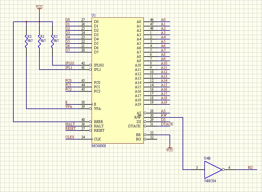
Nothing special to note here, except that some signals require pullups. The R/W* signal goes to an inverter, in order to have an active low RD signal. The active WR signal is R/W* itself.
GAL
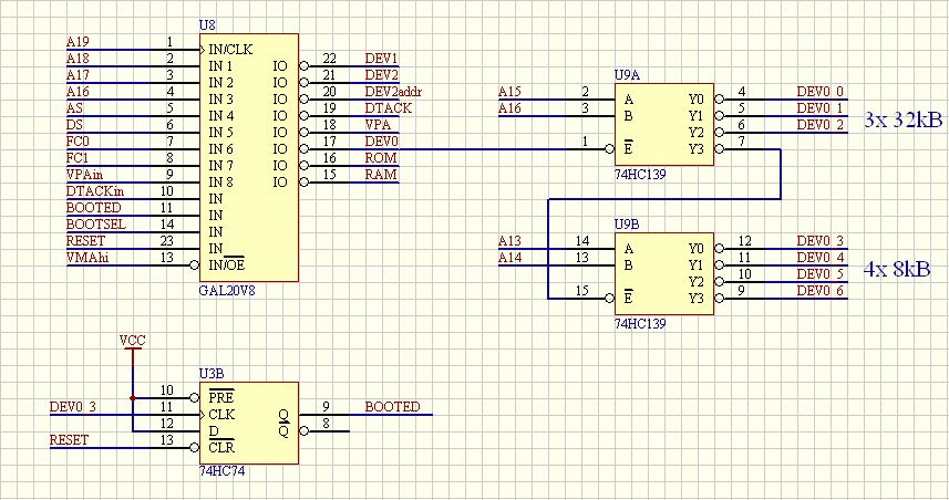
The address decoding section of the GAL generates the various chip select (CS) signals : RAM, ROM, DEV0, DEV1 and DEV2. As explained in the previous page, DEV0 is subdivided in 7 smaller chunks.
The GAL also generates the VPA signal, which is necessary to tell the 68000 that a synchronous bus cycle begins. This happens when DEV2 is selected.
Finally, the GAL takes 2 extra signals : BOOTED and BOOTSEL. We will talk about these signals later.
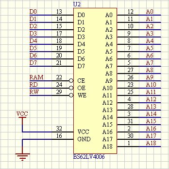
RAM
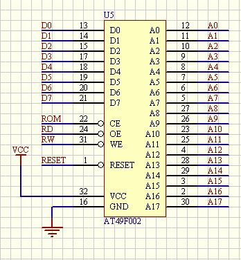
ROM/FLASH
PIC
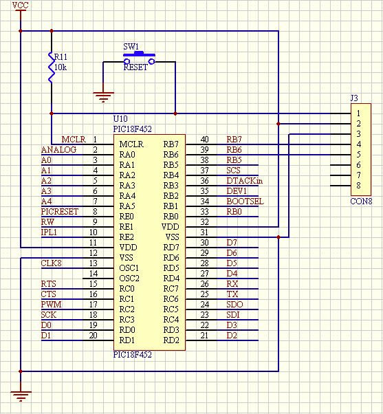
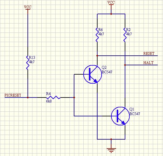
The PIC plays multiple roles on our board. First, it acts as a reset controller. The 68008 requires a long reset pulse after power-on. This pulse is generated by the PIC, at the cost of one pin. Note that the 68008 requires an open-collector driver for its RESET and HALT pins. Typically, a 74LS05 is used, but to save space on our PCB, 2 simple NPN transistors are used.
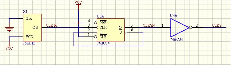
Clock generator
The CPU requires a 8MHz clock. This clock is also fed in the PIC18F, which multiplies it by 4 using its internal PLL.
Glue logic
The circuit below is the missing logic from the 68008 (version 48 pins). This comes directly from the Motorola datasheets.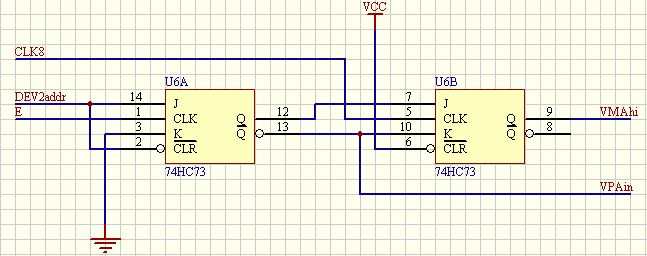
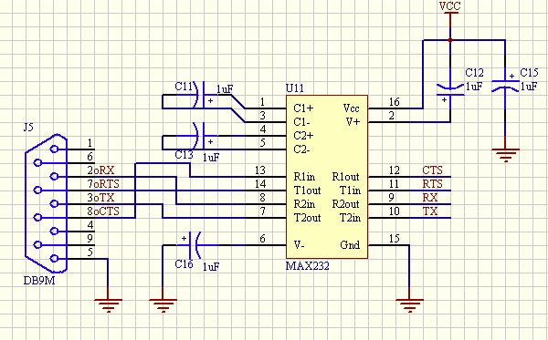
The RS232 driver, using a MAX232N
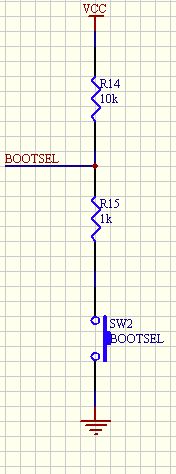
Boot selector.